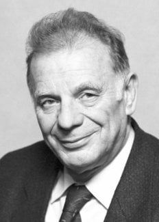
Zhores Alferov
Biographical
Life goes on surprisingly fast. It seems to happen a short time ago that I would attend anniversary celebrations in honour of noted physicists, my teachers who to my mind looked quite old. But at the present time, I myself have recently marked the 70th birthday.
My parents, Ivan Karpovich, and Anna Vladimirovna, had been Byelorussia born and raised. At the age of eighteen my father arrived in Saint Petersburg, in the year 1912. In his early hard years, he had been a docker, an errand boy and consequently got a job as a worker at the “Lessner” plant (later the Karl Marx Plant).
During World War I, he was a brave hussar, a non-commissioned officer of the Life Guards, a holder of the St. George Order. In September 1917, my father joined the Bolshevik party and retained his adherence to the socialist and communist principles to the end of his life.
In childhood, my brother and I “with a sinking heart” used to listen to father’s stories about the civil war and his military career. We learned how the formerly non-commissioned officer had been appointed to take command of a cavalry regiment in Red Army. Father also used to tell us about his meetings with revolutionary leaders: V.I. Lenin, L.D. Trotsky, B.E. Dumenko, “comrade Andrey” (A. Solts) who always put his apartment in the “Embankment House” at my father’s disposal while we stayed in Moscow. Father graduated from the Industrial Academy in 1935 and since then destiny was throwing us all over the country: Stalingrad, Novosibirsk, Barnaul, Syas’stroy in the environs of Leningrad, Turinsk (Sverdlovsk region), where we lived throughout the war time, and eventually the Minsk-city lying in ruins after the war. Dad was given a new assignment as director of a factory, joint enterprises (corporation of enterprises), later director of a trust. Mother headed a public organization of housewives; worked as a librarian and always remained our close friend while bringing us up without discouraging words. As a result of being so-called “director’s boys”, my brother and I tried to behave ourselves and to act in the way that people thought was correct and proper both at school and in public.
Learning was easy to me, and dependable defender, my elder brother Marx, made my existence cloudless at school and outdoors as well. Marx had graduated high school on June 21, 1941 (next day the Nazi invasion started) in the town of Syas’stroy and shortly after that we left for the Urals to Turinsk city as Dad had been assigned there to a post of director of a newly-built gunpowder cellulose factory (at the time referred to as factory No. 3). My elder brother, who was seventeen years old then, joined the Urals Industrial Institute (the Energy Faculty). The young student considered the problem of energy to be of cardinal importance for the future. But not long did he study at the Institute. He decided to defend his Motherland and to fight against fascists at the front line.
He passed Stalingrad, Kharkov, the Kursk battle. Having recovered after heavy head injury he was sent to the Army in the Field again. That was so called “another Stalingrad”, i.e., the Korsun-Shevchenko battle, where in his 20 years was shot down a Guard junior lieutenant Marx Ivanovich Alferov, my elder brother who remained of 20 years forever.
In October 1943, on the way to front from a hospital he spent 3 days with us in Sverdlovsk. I often look back and reflect on those three days; on his description of the war, his youthful enthusiasm and faith in the power of science, technology and human intelligence.
In the post-war particular situation I attended an only boy’s school in the destroyed Minsk-city, and was lucky in having an excellent physics teacher there Yakov Borisovich Meltserson. He delivered lectures on physics for us, rather naughty boys, and we were sitting quiet and listened attentively. The teacher loved physics devotedly and had a gift of making our imagination work. His explanation of the cathode oscilloscope operation and talk on radar systems greatly impressed me. When finishing the school I took his advice which institution to choose for education and that was a celebrated Ul’yanov Electrotechnical Institute in Leningrad (abbreviated to LETI).
Many of systematic studies in electronics and radio engineering that had been performed there made significant contributions into the electronics industry. As for me, it was my good fortune to meet my first supervisor there. Theoretical courses of studies were easy enough for me. It was the laboratory research that attracted me. Being a third-year student, I began to work in a laboratory of vacuum processes. My first investigations were directed by a research associate N.N. Sozina who studied semiconductor photodetectors. Since that time, half a century ago, semiconductors have become main objects of my scientific interests. A book “The Electroconductivity of Semiconductors” by F.F. Volkenshtein, which had been written in Leningrad (during the time of Leningrad’s siege) was my Textbook then. My graduation thesis was devoted to the problem of obtaining the thin films and investigating the photoconductivity of bismuth telluride compounds.
In December 1952, I graduated from the Institute and was offered by my supervisor N.N. Sozina to stay in the LETI to continue my study. But I dreamed of working at the Physico-Technical Institute that had been founded by Abram Fedorovich Ioffe. His book “Fundamentals of Modern Physics” was a manual for me. Happily, three vacancies for graduates had been given to us by Ioffe’s Institute. One of them fell to my lot. My joy was boundless. And may be it is this lucky distribution that has determined my happy scientific career.
In the letter to my parents, then residing in the Minsk-city, I wrote about my lucky chance. I did not know that Academician Ioffe was dismissed and left the Institute of which the director he had been for thirty years.
I recall my first day at the Physico-Technical Institute on January 30, 1953. I was introduced to my new supervisor, V.M. Tuchkevich, head of a subdivision. It was a very important problem to be solved by our not very big team: creation of germanium diodes and triodes (transistors) on p-n junctions.
The Physico-Technical Institute, being regarded on today’s scale, was not a big one. I was given an Institute pass No. 429, i.e., the total amount of employees was as high as the above mentioned number; most of famous physicists of the Physico-Technical Institute moved to Moscow (to I.V. Kurchatov’s, and newly-built atomic centers). Semiconductors elite followed A.F. Ioffe in order to work under his supervision in a recently organized semiconductor laboratory belonging to the Presidium of the Academy of Sciences of the USSR. In the Physico-Technical Institute there retained only D.N. Nasledov, B.T. Kolomiets and V.M. Tuchkevich as representatives of the old generation of physicists who formerly dealt with semiconductors.
Academician A.P. Komar was after A.E. Ioffe on charge of the Physico-Technical Institute. The new director’s attitude to his predecessor was not quite correct but as to the restoration and development of the Institute, his strategy was O.K. Of utmost importance was the support of works on the creation of new semiconductor electronics, space investigations (gas dynamics of high velocities and high temperature protective coatings; development of the light isotope separation methods for the hydrogen weapon (under the guidance of B.P. Konstantinov).
Studies of fundamental problems of physics, both theoretical and experimental ones, were encouraged too: just in this time experimental discovery of exciton was done (E.F. Gross), it was formulated the principles of a kinetic theory of strength (S.N. Zhurkov), development of the pioneering works on physics of atomic collisions were initiated (V.M. Dukel’skii, N.V. Fedorenko).
Both the director of the Institute (A.P. Komar) and the deputy director (D.N. Nasledov) understood the importance of drawing the interests of young people to science. It was a practice then to welcome newcomers at the highest level. In this way many renowned Russian scientists started their work, among them were present members of the Academy of Sciences, B.P. Zakharchenya, A.A. Kaplyanskii, E.P. Mazets, V.V Afrosimov and others.
I remember my first attendance of the seminar on semiconductors at the Physico-Technical Institute in February 1953 as one of the most impressive events I have ever experienced. That was a brilliant report delivered by E.F. Gross about the discovery of the exciton. The sensation I experienced then could not be compared to anything. I was stunned by the talk on the birth of a discovery in the area of science to which I myself had got the access.
Yet the main thing was everyday experimental work in the laboratory. Since that time I have been keeping, as a most precious thing, my laboratory daily report book that contains notes of mine about the creation of the first soviet p-n junction transistor on the 5th of March, 1953. And now, when recalling that time I cannot help feeling proud of what we had accomplished. We comprised a team of very young people. Under the guidance of V.M. Tuchkevich we succeeded in working out principles of the technology and the metrics of transistor electronics. Below are the names of researchers who had been working in our small laboratory: A.A. Lebedev, a Leningrad University graduate – the growth and doping of perfect germanium single crystals; Zh.I. Alferov – the preparation of transistors, their parameters being at the level of the best world samples; A.I. Uvarov and S. M. Ruvkin – the creation of a precise metrics of germanium single crystals and transistors; N.S. Yakovchuk, a graduate of the Faculty of Radio Engineering of the Leningrad Electrical Technical Institute – designing transistor-based circuits.
As early as in May 1953, the first Soviet transistor receivers were shown to the “top authorities”. That work, of which the performers had been working with passion peculiar to their young hearts and with utmost sense of responsibility, exerted a great influence upon me. While quickly and effectively progressing as a scientist, I began to comprehend the significance of the technology not only for electronic devices, but in basic research work too, in regard with notorious “minor” details and sporadic results. And it is since then that I prefer to analyze experimental result proceeding from “simple” general laws prior to putting forward sophisticated explanations.
In subsequent years, our team of researchers at the Physico-Technical institute expanded considerably and in a very short time the first Soviet germanium power rectifiers were created alongside with germanium photodiodes and silicon also were being carried out then.
In the month of May 1958, Anatolii Petrovic Alexandrov (later the President of the Academy of Sciences of the USSR) asked our team of working out a special semiconductor device for the first Soviet atomic submarine. That required a perfectly new technology and in addition to – another construction of germanium rectifiers, which had been done in a record short space of time. In the month of October, these devices were mounted on a submarine. I was a junior research associate at the Institute then, and was somewhat surprised by a telephone call from the first Vice-Chairman of the Government of the USSR, Dmitrii Fedorovich Ustinov, who asked me of fortnight reduction of the term. There was no getting away from that: I directly moved in the laboratory premises and settled there but, of course, the request was fulfilled that was my first State Order, which I had been decorated with then and which I valued very much.
In 1961, I read my candidate degree thesis that had been mainly devoted to working out and investigating of power germanium and partially silicon rectifiers. Occurrence of Soviet power semiconductor electronics became possible as a result of those works. Of great importance there, in the sense of a scientific, purely physical standpoint, had been a conclusion drawn by me that in p-i-n, p-n-n semiconductor homostructures under working current densities (for most of semiconductor devices), the current had been determined by recombination in heavily doped p- and n (n+)-regions while the recombination contribution in the middle i(n)-region of a homostructure was not the determining one: so, as soon as the first work on semiconductor lasers had appeared, it was natural for me to consider the advantages of employing in lasers the double heterostructure of p-i-n (p-n-n+, n-n-p+) type. The idea was formulated by us shortly after the appearance of the first work of R. Hall with co-workers, which described a semiconductor laser based on a GaAs homo-p-n-structure.
To realize principal advantages of heterostructures appeared to be possible only after obtaining of AlxGal-xAs heterostructures. We did that and it turned out that we had been only one month ahead in relation to American researches from IBM.
When we began investigating heterostructures, I used to convince my young colleagues, that we were not one and only group of scientists in the world who understood the significance of the concept that the semiconductor physics and electronics would be developing on the basis of HETERO-, rather than HOMO-structures. Indeed, since 1968 we entered an era of a strong competition and the first of all were three laboratories of the biggest American companies: Bell Telephone, IBM and RCA.
In 1967, while on a short trip to UK, I visited STL laboratories in Harlow. They were well equipped and the experimental base was excellent but English colleagues only discussed theoretical aspects of the heterostructures physics; they did not find experimental study of heterostructures to be promising then. In London I had some time for sightseeing and shopping. I bought there Wedding gifts to my fiancee Tamara Darskaya. As soon as I returned to Leningrad, we celebrated our wedding in a splendid restaurant “Krysha” (the Roof) in the Grand Hotel “Europe”.
Tamara was a daughter of a very popular actor of Voronezh Theater of Musical Comedy. Tamara worked then in the environs of Moscow at a big Space Enterprise under the guidance of Academician V.P. Glushko. She wonderfully combined incompatible beauty with cleverness and common sense and was always very kind toward her close friends. It was time of repeated weekly flights to Moscow. Holding a position of a Senior Research Associate at the Physico-Technical Institute, I could afford that. Leningrad-Moscow flight occurred in an hour time and the cost of a ticket to the TU-104 plane was as low as 11 rubles (about 15 US dollars). Nevertheless, after half a year shuttling between the two cities Tamara had moved to Leningrad.
In 1968-1969, we virtually realized all the ideas on control the electron and light fluxes in classical heterostructures based on the arsenid gallium-arsenid aluminum system. Apart from fundamental results that were quite new and important efficient one-side injection, the “superinjection” effect, diagonal tunneling, electron and optical confinement in a double heterostructure (which in a short while became the main element in studying the low-dimensional electron gas in semiconductors), we succeeded in employing principal benefits of heterostructure applications in devices, i.e., lasers, LEDs, solar cells, dynistors and transistors. Of utmost importance was, beyond doubts, the making of low threshold room temperature operating lasers on a double heterostructure (DHS) that had been suggested by us as far back as 1963. The approach developed by M.B. Panish and I. Hayashi (Bell Telephone) as well as by H. Kressel (RCA) was different from that of ours since they offered to use in lasers a single p-AlGaAs-p-GaAs heterostructure, which made their approach rather limited. A possibility of obtaining an efficient injection in the heterojunction seemed doubtful to them and, in spite of the fact that potential advantages of DHS had been recognized.
In August 1969, I first time visited the USA; my paper that I read there at the International Conference on Luminescence in Newarc (State of Delaver) was devoted to AlGaAs-based DHS low threshold room temperature lasers and produced an impression of an exploded bomb on American colleagues. Professor Ya. Pankov from RCA, who just shortly before my reading the paper had explained to me that they had not got a permission for my visiting their laboratory, as soon as I concluded my speech told me that the permission had been received. I could not help enjoying my refusal explaining that now I had been invited by that moment to attend IBM and Bell Telephone laboratories.
My seminar in the Bell followed by the looking over the laboratories and discussions with researches clearly revealed to me our merits and demerits of our progress in my laboratory. I believe that the soon commenced emulation for being the first in getting the continuous wave operation of laser at the room temperature was at that time a rare example of an open and friendly competition between laboratories belonging to the antagonistic Great Powers. We won the competition overtaking by a month Panish’s group in Bell Telephone. Significance of obtaining the continuous wave regime had the connection first and foremost with working out an optical fiber with low losses as well as the creation of our DHS lasers, which resulted in appearance and rapid development of optical fiber communication.
In the winter 1970-1971 and spring 1971, I spent six months in the USA working in laboratory of semiconductor devices at the University of Illinois together with Prof. Nick Holonyak. We met at the first time in 1967, when he visited my laboratory at the Physico-Technical Institute. Prof. Nick Holonyak, who is one of the founders of semiconductor optoelectronics, the inventor of the first visible semiconductor laser and LED became my closest friend. Now over 33 years we have discussed all semiconductor physics and electronics problems, political and life aspects and our interaction (visits, letters, seminars, telephone conversations) played very important role in our work and life.
In 1971, I became a recipient of the USA Franklin’s Institute gold medal for DHS laser works. Being my first international award, it was of particular value to me. There are Soviet physicists besides me who have been given the Franklin’s Institute gold medals too: Academician P.L. Kapitsa in 1944; Academician N.N. Bogolubov in 1974; Academician A.D. Sakharov in 1981. I consider it a big honour to belong to such a company!
An AlxGal-xAs system of lattice-matched heterostructures, which in practice seemed to be a lucky exception, was infinitely expanded on the basis of multi-component solid solutions, first theoretically and later on experimentally (InGaAsP is the most convincing example).
Heterostructure-based solar cells were created by us as far back as 1970. And when American scientists published their early works, our solar batteries have been already mounted on the satellites (sputniks) and their industrial production was in full swing. The cells, when being employed in space, proved their efficiency. For many years they have been operating on the “MIR” skylab and in spite of the fact that forecasts of a substantial decrease of the value of one watt of the electrical power have not been justified so far, the most effective energy source in space is, nevertheless, a set of solar cells on heterostructures of III-V compounds.
In 1972, my pupils-colleagues and I were awarded the Lenin’s Prize – the highest scientific Prize in the USSR. Our gladness regrettably was not cloudless. For some formal and obscure reasons we lost from the list of nominees R.F. Kazarinov and E.L. Portnoi.
On the day of the prize award I was in Moscow and called home, to Leningrad. But the telephone did not answer. Then, I called my parents (they have been living in Leningrad since 1963) and gladly told my father that I had been given the Lenin’s Prize. But my father replied – And so what- Our grandson is born today! In my lucky 1972 year, in addition to the prestigious prize I was elected a member of the Academy of Sciences. But the happiest day was that of Vanya Alferov’s birth.
Studies of superlattices and quantum wells were rapidly promoted in the West and afterwards in this country soon resulted in coming into being of a new area of the quantum physics of solid: the physics of low-dimensional electron systems. In this regard, studies of zero-dimensional structures – so-called “quantum dots” – form the summit of the above mentioned works. Gratifying is the circumstance that the Ioffe Institute today, while going through the hard times, remains the world leader in this area of physics. Works of the second and third generation of my students, those being well-known P.S. Kop’ev, N.N. Ledentsov, V.M. Ustinov, S.V. Ivanov have won general recognition nowadays. N.N. Ledentsov has become the youngest corresponding member of the Russian Academy of Sciences.
In 1987, I was elected director of the Ioffe Institute, in 1989, president of the Leningrad Scientific Center of the Academy of Sciences of the USSR; and in April 1990, Vice-President of the Academy of Sciences of the USSR. Afterwards, I was reelected and hold all these posts now within the Russian Academy of Sciences.
In the first years of my presidency and directorship we succeeded in remarkable scaling up research activity in our unique (for all the world) Academy of Sciences. We have also developed effective collaboration with Universities and Educational Institutions. The Physico-Technical Special Secondary School attached to Ioffe’s Physico-Technical Institute had been opened at that time; ongoing was the process of creation of specialized University chairs: the first one, that of Optoelectronics was organized in the Electrotechnical University, (formerly the LETI) as far back as in 1973. On the basis of both then existing and newly organized chairs a Physicotechnical faculty was set up in the Polytechnical Institute in 1988.
A great contribution into the above mentioned system makes the Scientific Educational Center that has been built by the Physico-Technical Institute and incorporates school boys, students and scientists in a magnificent edifice, which can be called “The Palace of Knowledge”.
Still, throughout the years passed, of greatest importance has been so far the existence of our Academy of Sciences as a unique both scientific and educational structure in Russia. The Academy faced the menace of abolition in the twenties as “an inheritance from the tsarist regime”. It faced the menace of abolition in the nineties as “an inheritance from the totalitarian Soviet regime”. To insure its safety I gave my consent to be a member of the Russian Parliament (a deputy of State Duma) in 1995. President Yu.S. Osipov and Vice-Presidents, Academicians and Corresponding Members, doctors and candidates of sciences, senior and junior research associates, lab-assistants and mechanics took a firm stand on this kind of situation. For the saving of the Academy of Sciences, we made compromises with the power but never with the conscience.
All that had been made by human beings, in principle, was made due to Science. And if our country’s choice is to be a Great Power, Russia will be the great power not because of the nuclear potential, not because of faith in God or president, or western investments but thanks to the labor of the nation, faith in Knowledge and Science and thanks to the maintenance and development of scientific potential and education.
When I was a little boy of ten, I have read a wonderful book “Two Captains” (by V. Kaverin). In essence, in my life I have been following the principle that was peculiar the main character of that book: “One should make efforts and search for. And having obtained whatever the purpose, to make efforts again”.
Of great importance here is to know what you are struggling for.
This autobiography/biography was written at the time of the award and later published in the book series Les Prix Nobel/ Nobel Lectures/The Nobel Prizes. The information is sometimes updated with an addendum submitted by the Laureate.
Zhores I. Alferov died on 1 March 2019.
Nobel Prizes and laureates
Six prizes were awarded for achievements that have conferred the greatest benefit to humankind. The 12 laureates' work and discoveries range from proteins' structures and machine learning to fighting for a world free of nuclear weapons.
See them all presented here.

