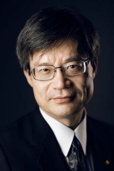
Hiroshi Amano
Biographical
I was born in Hamamatsu, Shizuoka Prefecture, Japan, on September 11, 1960, to my father Tatsuji and mother Yoshiko, and I grew up with younger brother Takashi. Hamamatsu is famous as the birthplace of Professor Kenjiro Takayanagi, a Japanese pioneer in the development of television, who succeeded in transmitting the first Katakana character “イ” by wireless transfer using a Braun tube in 1926, and also Soichiro Honda, who established Honda Motor Co., Ltd., in 1946. In addition, several engineering and manufacturing companies, such as motorbike companies, musical instrument companies, and optoelectronics companies, are based in Hamamatsu. A possible reason why I considered a career in engineering may have been the influence of growing up in such an industrial city.
I spent elementary school, junior high school, and high school at Hamamatsu. I was a weak child who was often ill. My grandmother Ken always nursed me, during which she often told me of her wretched experiences during World War II, so I learned a lot about the war. At elementary school, I concentrated on sports such as baseball and football. During elementary school and junior high school, I did not enjoy studying because the only reason to study seems to be to pass the entrance examination for high school. At high school, I had the same mathematics teacher for three years who taught me the importance of logical thinking and how to approach difficult problems in mathematics. I found that I could solve difficult problems if I thought logically. Although I became very interested in solving mathematics problems, I still did not have a good reason for studying.
I moved to Nagoya in 1979 to enter Nagoya University as a student of the Department of Electrical Engineering. In the introductory class to engineering, I heard a very profound interpretation of the meaning of the Kanji character “工,” which means engineering. The lecturer explained that the meaning of “工” is the connection of people with people, which means that the ultimate goal of engineering is to enrich the lives of people. I was astonished with this explanation and felt that my view of study had suddenly opened through recognizing that the meaning of study is to benefit the people. As a result, I became interested in all fields of study offered by my department, particularly computer science. This was soon after Bill Gates and Paul Allen established Microsoft (1975) and Steve Jobs and Stephen Wozniak started Apple Computers (1976). After the establishment of these now giant companies, the development of personal computer (PC) systems proceeded rapidly, and I hoped to contribute to the further development of PC systems.
In 1982, when I was in my third year of university, I had to choose a dissertation research topic. Unfortunately, there were no topics concerning computer science, especially the design of central processing units. But when I found that GaN-based blue LEDs could be researched in Professor Isamu Akasaki’s laboratory, I decided to pursue this topic as my dissertation topic. At that time, Braun tubes were used as the monitors of PCs and also in television systems. Because Braun tubes were so large, I thought that if I could develop blue LEDs, I could change the world by improving people’s lives by providing the means to develop more smart PC and TV systems. At that time, I did not know how difficult it would be to develop blue LEDs.
At that time, funding of our laboratory was very limited. Therefore, the students at Nagoya University had to develop their own system to enable the growth of nitride crystals by metal-organic vapor phase epitaxy (MOVPE). Through the efforts of a master’s degree student followed by myself and Mr Koide, a student in the year above me, we succeeded in developing an MOVPE system. I then used our laboratory-built MOVPE system to try to grow high-quality GaN, and Mr. Koide focused on growing AlN and AlGaN. However, the growth of GaN on a foreign substrate such as sapphire was so difficult that I spent three years in vain trying to grow high-quality GaN.
In February 1985, almost at the end of my master’s course, I was still carrying out lonely fruitless experiments. When I compared my GaN and AlN grown by Mr Koide, I found that the surface morphology of his AlN was slightly better that that of my GaN, so I decided to deposit AlN just before growing GaN. I noticed that a very high temperature was necessary to grow AlN. However, the heating system of our MOVPE system was so old that it could not reach the required temperature. I then remembered a discussion with Dr. Sawaki, at that time Associate Professor at Akasaki Laboratory. He said that in the growth of boron phosphide (BP) on Si for which the lattice mismatch is 16%, almost the same as that of GaN on sapphire, the predeposition of P was effective for growing BP with a flat surface. He also mentioned that a P cluster should act as a nucleation center causing BP to grow laterally in the initial stage. I decided to deposit a very small amount of AlN at a low temperature, which I anticipated would act as a nucleation center. When I took the resulting sample out from the MOVPE reactor, I first thought that I had forgotten to supply the Ga source. But when I checked the surface morphology using an optical microscope, I finally recognized that I had succeeded in growing GaN with an atomically flat surface. It took almost one year for this result to be published in Applied Physics Letters because I had to check not only the surface morphology but also the crystalline quality, electrical properties and optical properties. I found that all the properties of the GaN film were far superior to those reported previously. This process is called low-temperature deposited buffer layer technology for growing GaN on a sapphire substrate by MOVPE.
Our next challenge for us was to realize p-type GaN. I unsuccessfully tried to grow p-type GaN using Zn as an acceptor dopant from 1985 to 1988. At NTT, where I spent the internship of my PhD, I found that blue luminescence increased irreversibly when Zn-doped GaN was irradiated with electrons. I called this low-energy electron beam irradiation (LEEBI) treatment. However, even after LEEBI treatment, the Zn-doped samples did not show p-type conduction. In 1989, I became a Research Associate of Akasaki laboratory before completing my PhD. When I read the book “Bonds and Bands in Semiconductors” written by J. C. Phillips, I found that Mg is a better acceptor impurity than Zn in GaP. Then, myself and Mr. Kito, a master’s student, started to investigate the Mg doping of GaN. We found that grown Mg-doped GaN showed high resistivity, but after LEEBI treatment, it showed distinct p-type conduction. We also succeeded in fabricating the world’s first pn-junction-type UV/blue LED. In 1991 Nichia Chemicals team led by Dr. Nakamura found that p-type GaN could be grown by simple thermal annealing, which became the de fact standard method for the growth of p-type GaN.
In 1992, I moved to the School of Science and Technology, Meijo University, to work with Professor Akasaki, where I became an Assistant Professor. In 1998 and 2002, I became an Associate Professor and a Professor, respectively. In 2010, I moved to the Engineering Department, Nagoya University, where I continued to work as a Professor. I have been Director of Akasaki Research Center, Nagoya University, since 2011.
I was awarded several honors such as the IEEE/LEOS Engineering Achievement Award in 1996; the Rank Prize, Rank Prize Foundation, UK, in 1998; the Marubun Academic Award, Marubun Research Promotion Foundation, Japan, in 2002; the Takeda Award, Takeda Foundation, Japan, in 2002; the Japanese
Association for Crystal Growth JACG Award, Japan, in 2008; the NISTEP Award, National Institute of Science and Technology Policy, Japan, in 2009; the Order of Culture from the Japanese Emperor in 2014; and the Nobel Prize in Physics, Nobel Foundation, Sweden, in 2014.
I have been a fellow of the Japan Society of Applied Physics (JSAP) since 2009 and a fellow of the Institute of Physics (IOP), UK, since 2011. I am also a member of several academic organizations.
Selected activities include Sub Chair of the Program Committee of the International Symposium on Compound Semiconductors in 2007, Program Committee Chair of the Second International Symposium on the Growth of Nitride semiconductors in 2010, Program Committee Chair of the Third International Symposium on Growth of Nitride Semiconductors in 2012, and Organizing Committee Chair of the International Workshop on Nitride Semiconductors in 2012.
This autobiography/biography was written at the time of the award and later published in the book series Les Prix Nobel/ Nobel Lectures/The Nobel Prizes. The information is sometimes updated with an addendum submitted by the Laureate.
Nobel Prizes and laureates
See them all presented here.