Popular information
Information for the public:
The masters of light (pdf)
Populärvetenskaplig information:
Ljusets mästare (pdf)

The Nobel Prize in Physics 2009
The 2009 Nobel Prize in Physics honors three scientists, who have had important roles in shaping modern information technology, with one half to Charles Kuen Kao and with Willard Sterling Boyle and George Elwood Smith sharing the other half. Kao’s discoveries have paved the way for optical fiber technology, which today is used for almost all telephony and data communication. Boyle and Smith have invented a digital image sensor – CCD, or charge-coupled device – which today has become an electronic eye in almost all areas of photography.
The masters of light
When the Nobel Prize in Physics is announced in Stockholm, a large part of the world receives the message almost instantly. At almost the speed of light, the highest of speeds, the message is spread around the world. Text, images, speech and video are shuffled around in optical fibers and through space, and are received instantly in small and convenient devices. It is something that many people have already come to take for granted. The optical fiber has been a prerequisite for this extremely rapid development in the field of communications, a development that Charles Kao predicted over 40 years ago.

Just a few years later, Willard Boyle and George Smith radically altered the conditions for the field of photography, because film is no longer needed in cameras where the images can be captured electronically with an image sensor. The electronic eye, the CCD, became the first truly successful technology for the digital transfer of images. It opened the door to a daily stream of images, which is filling up the optical fiber cables. Only optical fiber is capable of transferring such large quantities of data that electronic image sensor technology yields.
The arrival of light
It is via sunlight that we see the world. However, it would take a long time before humans acquired the skills to control light and direct it into a waveguide. In this way coded messages could be transmitted to many people simultaneously.
This development required numerous inventions, big and small, which form the foundations for the modern information society. The optical fiber required modern glass technology in order to be developed and manufactured. A reliable source of light was also needed and this was provided by semiconductor technology. Finally, an ingenious network needed to be assembled and extended, consisting of transistors, amplifiers, switches, transmitters and receivers, as well as other units, all working together. The telecommunications revolution was made possible by the work of thousands of scientists and inventors from all around the world.
Playing with light
The 1889 World Exhibition in Paris celebrated the centenary of the French revolution. The Eiffel tower was to become one of the most well-known monuments of this exhibition. However, a remarkable play of lights proved a less memorable spectacle. It was performed with water fountains filled with colorful beams of light. This show was made possible with electricity. A source of inspiration was also provided by earlier attempts, in the middle of the 19th century, to create beams of light guided by water. Those trials had shown that when a beam of water is exposed to sunlight, the light travels through the beam and follows its curving shape.
Of course, the effects of light in glass or water had been discovered much earlier than that. Already 4 500 years ago, glass was manufactured in Mesopotamia and Egypt. The Venetian glass masters could not have been ignorant of the beautiful play of light that occurred in their swirling decorations. Cut glass was used in candelabras and crystal chandeliers, and the elusive mystery of the rainbow challenged the imagination of many men and women long before the laws of optics provided the answer in the 17th century. However, it was only about 100 years ago that these ideas surfaced and people tried to make use of captured beams of light.
Capturing light
A ray of sunlight that falls into water bends when it hits the surface, because the so-called refractive index of water is higher than the refractive index of air. If the direction of the light beam is inverted, travelling from water into air, it is possible that it will not enter the air at all, and instead will be reflected back into the water. This phenomenon forms the basis for optical waveguide technology where light is captured inside a fiber with a higher refractive index than its surrounding environment. A ray of light that is directed into a fiber, bounces against the glass wall and moves forward since the refractive index of glass is higher than the surrounding air (figure 2).

The medical profession has used short and simple optical fibers since the 1930s. With a bundle of thin glass rods, they could peek inside the stomachs of patients or highlight teeth during operations. However, when the fibers touched each other they leaked light, and they also easily became worn out. Coating the bare fiber in a glass cladding with a lower refractive index led to considerable improvements, which in the 1960s paved the way for industrial manufacturing of instruments for gastroscopy and other medical uses.
For long distance communication, however, these glass fibers were useless. Furthermore, few were really interested in optical light; these were the days of electronics and radio technology. In 1956, the first transatlantic cable was deployed, and it had a capacity for 36 simultaneous phone calls. Soon satellites would begin to cover the growing communication needs – telephony increased dramatically and television broadcasting required ever higher transfer capacities. Compared to radio waves, infrared or visible light carries tens of thousands times more information, so the potential of optical light waves could not be disregarded any longer.
Transmitting light
The invention of the laser at the beginning of the 1960s was a decisive step forward for fiber optics. The laser was a stable source of light that emitted an intensive and highly focused beam of light, and could be pumped into a thin optical fiber. The first lasers emitted infrared light and required cooling. Around 1970 more practical lasers were developed which could work continuously at room temperature. This was a technological breakthrough that facilitated optical communication.
All information could now be coded into an extremely fast flashing light, representing digital ones and zeros. However, how such signals could be transmitted over longer distances was still not known – after just 20 meters, only 1 percent of the light that had entered the glass fiber remained.
Reducing this loss of light became a challenge for a visionary like Charles Kuen Kao. Born in 1933 in Shanghai, he had moved to Hong Kong together with his family in 1948. Educated as an electronics engineer, he defended his Ph.D.-thesis in 1965 in London. By that time he was already employed at the Standard Telecommunication Laboratories, where he meticulously studied glass fibers together with his young colleague George A. Hockham. Their goal was that at least 1 percent of the light that entered a glass fiber would remain after it had travelled 1 kilometer.
In January 1966, Kao presented his conclusions. It was not imperfections in the fiber thread that was the main problem, instead it was the glass that had to be purified. He admitted that this would be feasible but very difficult. The goal was to manufacture glass of a transparency that had never been attained before. Kao’s enthusiasm inspired other researchers to share his vision of the future potential of fiber optics.
Glass is manufactured from quartz, the most abundant mineral on Earth. During its production, different additives such as soda and lime are used in order to simplify the process. However, in order to produce the purest glass in the world, Kao pointed out that fused quartz, fused silica, could be used. It melts at almost 2 000 °C, a heat difficult to control but from which one would draw out ultra-thin threads of fiber.
After four years, 1971, scientists at the Corning Glass Works in the USA, a glass manufacturer with over 100 years experience, produced a 1 kilometer long optical fiber using chemical processes.
Filled with light
Ultra-thin fibers made out of glass may seem very fragile. However, when glass is correctly drawn out in a long thread, its properties change. It becomes strong, light and flexible, which is a prerequisite if the fiber is to be buried, drawn under water or bent around corners. Unlike copper cables, glass fiber is not sensitive to lightning, and unlike radio communication, it is not affected by bad weather.
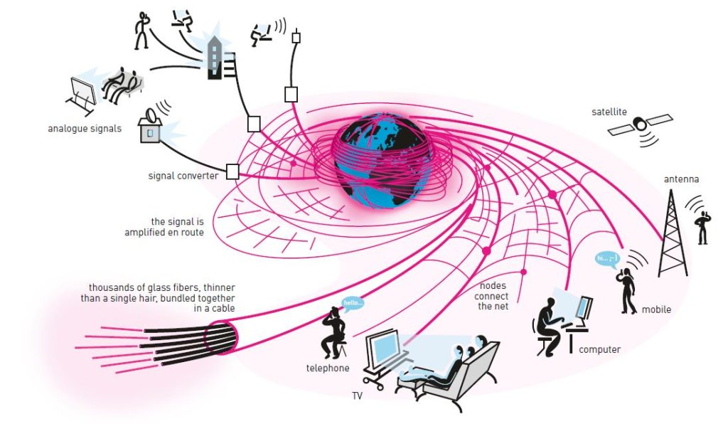
It took a fair share of time to coil the Earth in fiber. In 1988, the first optical cable was laid out along the bottom of the Atlantic Ocean between the United States and Europe. It was 6 000 km long. Today, telephone and data communication flows in a network of optical glass fiber, the length of which totals over 1 billion km. If that amount of optical fiber was wrapped around the globe it would span the world more than 25 000 times – and the amount of fiber is increasing every hour (figure 1).
Even in a high purity glass fiber, the signal is slightly reduced along the way and has to be reinforced when it is transmitted over longer distances. This task, which previously required electronics, is today performed by optical amplifiers. This has brought an end to unnecessary losses that occur when light is transformed to and from electronic signals.
Today 95 percent of the light remains after having been transmitted a full kilometer, a number that should be compared to Kao’s ambition of having 1 percent left after that same distance. Furthermore, it is not possible to speak of only one single kind of fiber. Choosing which fiber to use is subject to many different technical considerations, communication needs and costs.
The fibers consist of a sophisticated interplay between size, material properties, and wavelengths of light. Semiconductor lasers and light diodes the size of a grain of sand fill networks of optical fibers with light which carries almost all of the telephone and data communication around the world. Infrared light with a wavelength of 1.55 micrometers, is nowadays used for all long distance communication where the losses are lowest.
The capacity of optical cable networks is still growing at an amazing speed – transferring thousands of gigabits per second is no longer a dream. Technological development is heading in the direction of more and more interactive communication, where optical fiber cables are designed to reach all the way into the homes of each and every one of us. The technology already exists. What we do with it is an altogether different question.
Electronic eye
Sometimes inventions appear totally unanticipated. The image sensor, CCD, or chargecoupled device, is such an invention. Without the CCD, the development of digital cameras would have taken a slower course. Without CCD we would not have seen the astonishing images of space taken by the Hubble space telescope, or the images of the red desert on our neighboring planet Mars.
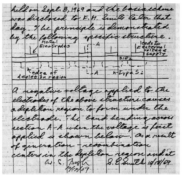
This was not what the inventors of the CCD, Willard Boyle and George Smith, had imagined when they began their work. One day in September 1969, they outlined the basis of an image sensor on a blackboard in Boyle’s office. At that time they did not have photographic images in mind. Their aim with the CCD was to create a better electronic memory. As a memory device it is now forgotten. However, they did come up with an indispensable part of modern imaging technology. The CCD is yet another success story of our electronic era.
Images become digital
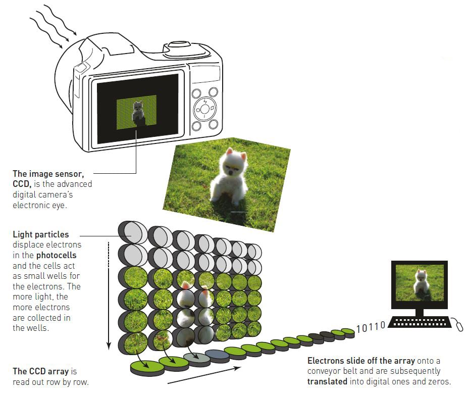
Just like many other devices in the electronics industry, a digital image sensor, CCD, is made out of silicon. The size of a stamp, the silicon plate holds millions of photocells sensitive to light. The imaging technique makes use of the photoelectric effect which was first theorized by Albert Einstein and earned him 1921’s Nobel Prize. The effect occurs when light hits the silicon plate and knocks out electrons in the photocells. The liberated electrons are gathered in the cells which become small wells for them. The larger the amount of light, the larger the number of electrons that fill these wells.
When voltage is applied to the CCD array, the content of the wells can be progressively read out; row by row, the electrons slide off the array onto a kind of a conveyor belt (figure 3). So for example, an array of 10 x 10 image points is transformed into a 100 points long chain. In this manner the CCD transforms the optical image into electric signals that are subsequently translated into digital ones and zeros. Each cell can then be recreated as an image point, a pixel. When the width of a CCD, expressed in pixels, is multiplied with its height, the image capacity of the sensor is obtained. Thus a CCD with 1280 x 1024 pixels yields a capacity of 1.3 megapixels (1.3 million pixels).

The CCD renders an image in black and white, so various filters have to be used in order to obtain the colors of light. One kind of filter that contains one of the base colors red, green or blue, is placed over every cell in the image sensor. Owing to the sensitivity of the human eye, the number of green pixels needs to be twice that of the blue or red pixels. For more advanced imaging, a number of filters may be used.
Challenges at work
The fact that Boyle and Smith got the idea for the CCD during their short brainstorming session 40 years ago can be attributed to the internal politics of their employer. Their boss at Bell Labs outside New York, encouraged them to take on the challenge and enter a competition regarding the development of a better bubble memory, another one of the Bell Labs’ inventions. When the basic design for the CCD was finished, it would only take a week before technicians assembled the first prototype. As a memory it is long forgotten, but the CCD has become the center of many digital imaging techniques.

The American George Smith was hired at Bell Labs in 1959, and took out 30 patents during his time at the company. When he retired in 1986, he could at last dedicate himself fully to his life-long passion – sailing on the great seas, which has brought him around the globe many times.
By 1969, Willard Boyle had made many important discoveries, for instance in relation with the development of the world’s first continuous red light laser. Boyle was born in a distant part of Nova Scotia in Canada, and was educated at home by his mother until the age of 15. He began to work at Bell Labs in 1953, and in the 1960s he joined the 400 000 scientists in the USA whose efforts were to put the first man on the moon on 20 July 1969.
A photographic camera for everyone
The advantages of the electronic image sensor quickly became evident. In 1970, just about a year after the invention, Smith and Boyle could demonstrate a CCD in their video camera for the first time. In 1972, the American company Fairchild constructed the first image sensor with 100 x 100 pixels, which entered production a few years later. In 1975, Boyle and Smith themselves constructed a digital video camera of a sufficiently high resolution to manage television broadcasts.
It would not be until 1981 before the first camera with built-in CCD appeared on the market. Not withstanding its bulky and primitive characteristics, when compared to contemporary cameras, it initiated a more commercially oriented digitalization in the field of photography. Five years later in 1986, the first 1.4 megapixel image sensor (1.4 million pixels) arrived, and a further nine years on in 1995, the world’s first fully digital photographic camera appeared. Camera manufacturers around the world quickly caught on, and soon the market was flooded with ever smaller and cheaper products.
With cameras equipped with image sensors instead of film, an era in the history of photography had ended. It had begun in 1839 when Louis Daguerre presented his invention of photographic film before the French Académie des Sciences.
When it comes to everyday photography, digital cameras have turned out to be a commercial success. Lately the CCD has been challenged by another technology, CMOS, or Complementary Metal Oxide Semiconductor; a technology that was invented at about the same time as CCD. Both make use of the photoeffect, but while the electrons gathered in a CCD march in line in order to be read out, every photocell in a CMOS is read out on site.
CMOS consumes less energy so batteries last longer, and for a long time it has also been cheaper. However, one also has to take into account its higher noise levels and the loss of image quality, and consequently CMOS is not sufficiently sensitive for many advanced applications. CMOS is currently often used for everyday cell phone photography, and for other kinds of photography. Both technologies, however, are constantly being developed and for many applications they are interchangeable.
Three years ago, CCD breached the limit of 100 megapixels, and although the image quality is not only dependent on the number of pixels, surpassing this limit is seen to have brought digital photography a further step into the future. There are those that predict that the future belongs to CMOS rather than to CCD. Others still, maintain that the two technologies will continue to supplement each other for a long time.
Light-sensitive pixels
Initially, no one predicted that CCD would become indispensable to the field of astronomy. However, it is precisely thanks to digital technology that the wide-angle camera on the Hubble space telescope can send the most astonishing images back to Earth (figure 5). The camera’s sensor initially consisted of only 0.64 megapixels. However, as four sensors were interconnected, they provided a total of 2.56 megapixels. This was a big thing in the 1980s when the space telescope was designed. Today the Kepler satellite has been equipped with a mosaic sensor of 95 megapixels, and the hope is that it will discover Earth-like planets around stars other than the sun.

Early on, astronomers realized the advantages of the digital image sensor. It spans the entire light spectrum, from X-ray to infrared. It is a thousand times more sensitive than photographic film. Out of 100 incoming light particles a CCD catches up to 90, whereas a photographic plate or the human eye will only catch one. In a few seconds, light from distant objects is gathered – a process that previously would have taken several hours. The effect is also directly proportional to the intensity of the light – the larger the amount of light, the higher the number of electrons.
In 1974 the first image sensor had already been used to take photographs of the moon – the first astronomical images ever to be taken with a digital camera. With lightning speed, astronomers adopted this new technology; in 1979 a digital camera with a resolution of 320 x 512 pixels was mounted on one of the telescopes at Kitt Peak in Arizona, USA,
Today whenever photo, video or television is used, digital image sensors are usually involved in the process. They are useful for surveillance purposes both on Earth and in space. Furthermore, CCD technology is used in a host of medical applications, e.g. imaging the inside of the human body, both for diagnostics and for surgical operations. The digital image sensor has become a widely used instrument at the service of science both at the bottom of the oceans and in space. It can reveal fine details in very distant and in extremely small objects. In this way, technological and scientific breakthroughs intertwine.
LINKS AND FURTHER READING
Popular science
Smith, G.E. (2009) The invention and early history of the CCD. Nuclear Instruments and Methods in Physics Research A, 607, p. 1–6.
Janesick, J.R. (2002) Duelling Detectors. SPIE’s oemagazine, February, p. 30-33.
Janesick, J.R. (2001) Scientific Charge-Coupled Devices. SPIE Press Monograph, Vol. PM83.
Hecht, J. (1991) City of Light: The Story of Fiber Optics. Oxford University Press.
Su, F. (1990) Technology of our times: people and innovation in optics and optoelectronics. SPIE Press, p. 80–95.
Scientific articles
Kao, C.K. , Hockham, G.A. (1966) Dielectric-fibre Surface Waveguides for Optical Frequencies. Proceedings of the Institution of Electrical Engineers-London 113, p. 1151.
Boyle, W.S., Smith, G.E. (1970) Charge Couple Semiconductor Devices. Bell System Technical Journal 49, p. 587.
Links
www.fiber-optics.info
www.jyi.org/volumes/volume3/issue1/features/peterson.html
THE LAUREATES
CHARLES KUEN KAO
Happy Valley, Hong Kong
China
https://ethw.org/Oral-History:Charles_Kao
British and US citizen. Born 1933 in Shanghai, China. Ph.D. in Electrical Engineering 1965 from University of London, UK.
Director of Engineering of Standard Telecommunication Laboratories, Harlow, UK.
Vicechancellor, Chinese University of Hong Kong. Retired 1996.
WILLARD STERLING BOYLE
Wallace, Nova Scotia
Canada
www.science.ca/scientists/scientistprofile.php?pID=129
Canadian and US citizen. Born 1924 in Amherst, NS, Canada. Ph.D. in Physics 1950 from McGill University, QC, Canada.
Executive Director of Communication Sciences Division, Bell Laboratories, Murray Hill, NJ, USA. Retired 1979.
GEORGE ELWOOD SMITH
Barnegat, New Jersey
USA
www.ieeeghn.org/wiki/index.php/Oral-History:George_E_Smith
US citizen. Born 1930 in White Plains, NY, USA. Ph.D. in Physics 1959 from University of Chicago, IL, USA.
Head of VLSI Device Department, Bell Laboratories, Murray Hill, NJ, USA. Retired 1986.
© The Royal Swedish Academy of Sciences
Nobel Prizes and laureates
Six prizes were awarded for achievements that have conferred the greatest benefit to humankind. The 14 laureates' work and discoveries range from quantum tunnelling to promoting democratic rights.
See them all presented here.
